Detailed Description
On this page
Hardware Overview
The figure below illustrates the various hardware components that are located on the top-side of the M.2 M-key Stack FMC.
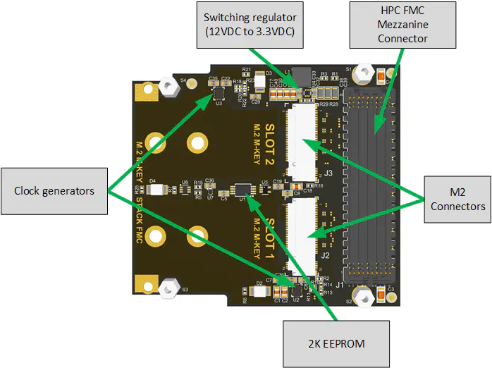
The main components on the top-side of the mezzanine card are:
- 2x M-key M.2 socket connectors (for the SSDs)
- High Pin Count FMC Mezzanine Connector
- 2K EEPROM
- 2x PCIe Clock oscillators (100MHz)
- Switching regulator
The figure below illustrates the various hardware components that are located on the bottom-side of the mezzanine card.
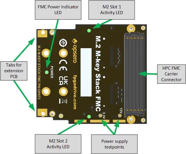
The main components on the bottom-side of the mezzanine card are:
- High Pin Count FMC Carrier connector
- FMC Power indicator LED
- M.2 module activity LEDs
- Test points for power supplies
Stack FMC concept
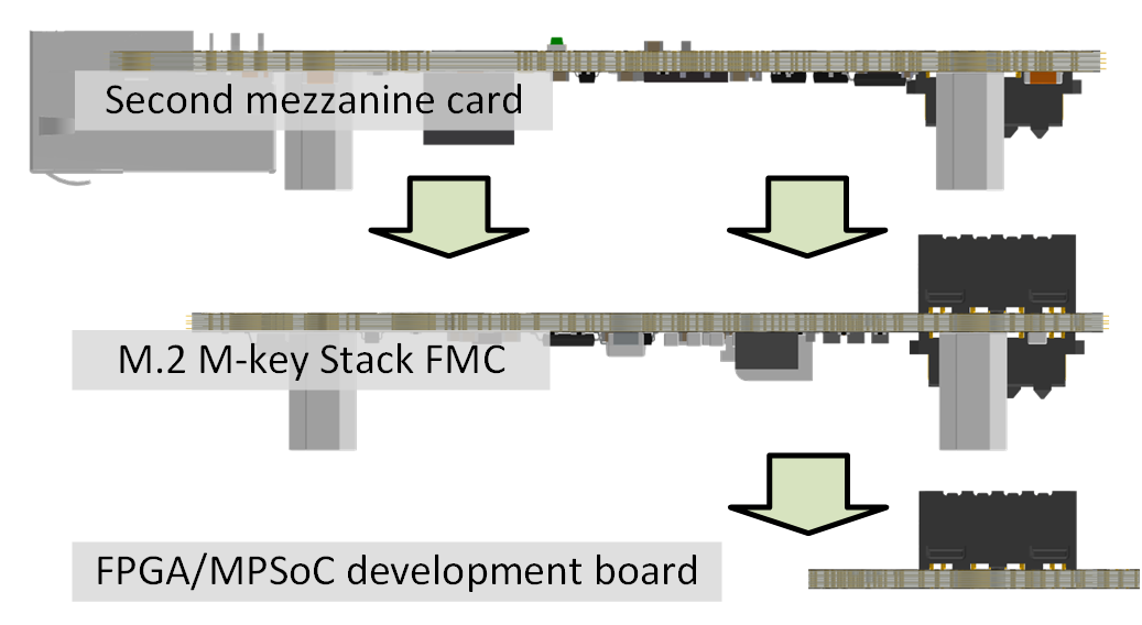
With the M.2 M-key Stack FMC, Opsero introduces the Stack FMC concept whereby a single FMC slot of the FPGA/MPSoC development board can be shared by two mezzanine cards. Many FMC cards do not make use of all of the I/O that is provided by the FMC carrier board. Normally, when using such FMC cards, the unused I/Os are not accessible and this removes from the potential applications of the FPGA/MPSoC device. Opsero’s new range of Stack FMCs offer a solution to this problem, by proposing a standard method for partitioning the FMC I/Os and power supplies between two mezzanine cards.
Opsero Stack FMCs are mezzanine cards that have a carrier-side FMC connector on the side of the board that is opposite the mezzanine-side FMC connector. The carrier-side FMC connector mates with a second mezzanine card. A complete stack (see image below) consists of the FPGA/MPSoC development board at the bottom, followed by the first level mezzanine card (the Stack FMC) with the second level mezzanine card on the top.
Power and I/O partitioning
The partitioning of power and I/O between a Stack FMC and a second mezzanine card was designed with the objective of achieving compatibility with the greatest number of existing FMC cards, while respecting the limits of the VITA 57.1 standard as much as possible.
Power
It cannot be expected that the power capacity of a single FMC slot be able to supply two FMC cards if there is no intelligent partitioning of the power supplies. A Stack FMC satisfies the majority of it’s power needs from the +12VDC power supply, and passes the main power supplies +3.3VDC and VADJ up for exclusive use by the second mezzanine card. A Stack FMC also uses the +3.3VAUX supply, however only ever drawing a few milliamps from it. The +12VDC and +3.3VAUX supplies are also passed up to the second mezzanine card. The diagram below illustrates the power partitioning in a complete stack.
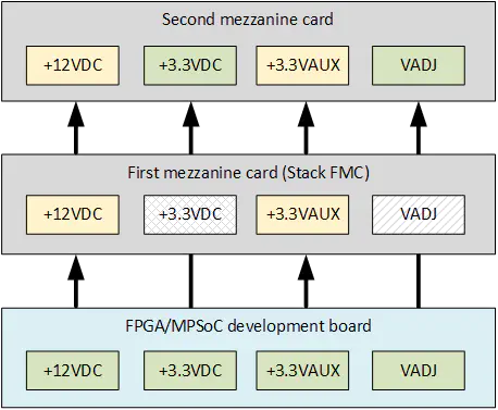
- A grey shaded box indicates that the supply is not available on that level
- A yellow box indicates that the supply is shared by both levels
- A green box indicates that the supply is exclusively available to that level
I/O
The I/O partitioning was designed with the objective that the Stack FMC could accomodate the greatest number of existing FMC cards as second mezzanine. As such, all of the I/O signals are passed through to the second mezzanine, with the exception of the gigabit transceivers and their associated clocks. This choice comes with the limitation that the second mezzanine does not have access to any gigabit transceivers, and that the Stack FMC requires an on-board I2C I/O expander to satisfy all of it’s low-speed I/O needs (if any). Naturally, the I2C bus is shared between the two mezzanine cards. The diagram below illustrates the partitioning of the I/O signals in a complete stack.
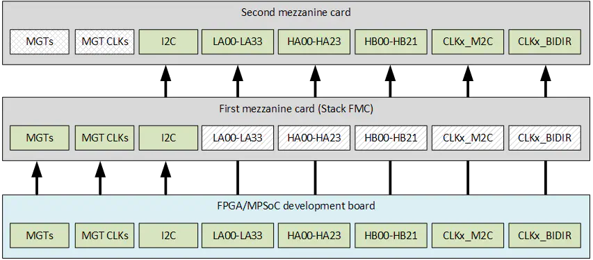
- A grey shaded box indicates that the I/Os are not available on that level
- A green box indicates that the I/Os are exclusively available to that level
M.2 connectors
The M.2 M-key modules connect to the mezzanine card through 2x M-key M.2 connectors ( Amphenol, PCIe M.2 connector, MDT420M02003 ).
The pinout of the M.2 connector is shown in the table below:
| Pin # | Pin name | Connection | Pin # | Pin name | Connection |
|---|---|---|---|---|---|
| 1 | GND | GND | 2 | 3.3V | 3V3 |
| 3 | GND | GND | 4 | 3.3V | 3V3 |
| 5 | PER-N3 | SSD2FPGA_3_N | 6 | N/C | NC |
| 7 | PER-P3 | SSD2FPGA_3_P | 8 | N/C | NC |
| 9 | GND | GND | 10 | DAS/DSS#/LED1# | DAS/DSS# |
| 11 | PET-N3 | FPGA2SSD_3_N | 12 | 3.3V | 3V3 |
| 13 | PET-P3 | FPGA2SSD_3_P | 14 | 3.3V | 3V3 |
| 15 | GND | GND | 16 | 3.3V | 3V3 |
| 17 | PER-N2 | SSD2FPGA_2_N | 18 | 3.3V | 3V3 |
| 19 | PER-P2 | SSD2FPGA_2_P | 20 | N/C | NC |
| 21 | GND | GND | 22 | N/C | NC |
| 23 | PET-N2 | FPGA2SSD_2_N | 24 | N/C | NC |
| 25 | PET-P2 | FPGA2SSD_2_P | 26 | N/C | NC |
| 27 | GND | GND | 28 | N/C | NC |
| 29 | PER-N1 | SSD2FPGA_1_N | 30 | N/C | NC |
| 31 | PER-P1 | SSD2FPGA_1_P | 32 | N/C | NC |
| 33 | GND | GND | 34 | N/C | NC |
| 35 | PET-N1 | FPGA2SSD_1_N | 36 | N/C | NC |
| 37 | PET-P1 | FPGA2SSD_1_P | 38 | DEVSLP | GND |
| 39 | GND | GND | 40 | SMB_CLK | NC |
| 41 | PER-N0 | SSD2FPGA_0_N | 42 | SMB_DATA | NC |
| 43 | PER-P0 | SSD2FPGA_0_P | 44 | ALERT# | NC |
| 45 | GND | GND | 46 | N/C | NC |
| 47 | PET-N0 | FPGA2SSD_0_N | 48 | N/C | NC |
| 49 | PET-P0 | FPGA2SSD_0_P | 50 | PERST# | PERST# |
| 51 | GND | GND | 52 | CLKREQ# | NC |
| 53 | REFCLK-N | REFCLK_SSD_N | 54 | PEWAKE# | NC |
| 55 | REFCLK-P | REFCLK_SSD_P | 56 | RSVD | NC |
| 57 | GND | GND | 58 | RSVD | NC |
| 67 | N/C | NC | 68 | SUSCLK | NC |
| 69 | PEDET | PEDET | 70 | 3.3V | 3V3 |
| 71 | GND | GND | 72 | 3.3V | 3V3 |
| 73 | GND | GND | 74 | 3.3V | 3V3 |
| 75 | GND | GND |
HPC FMC Mezzanine Connector
The M.2 M-key Stack FMC has a high pin count (HPC) FMC (FPGA Mezzanine Card) connector for interfacing with an FPGA or SoC development board. The part number of this connector is Samtec, High pin count FMC connector, Module side, ASP-134488-01 . This HPC FMC connector can be mated with LPC, HPC or FMC+ carrier connectors.
The pinout of this connector conforms to the VITA 57.1 FPGA Mezzanine Card Standard (for more information, see Pin configuration. For more information on the FMC connector and the VITA 57.1 standard, see the Samtec page on VITA 57.1 .
HPC FMC Carrier Connector
The mezzanine card has a HPC FMC Carrier-side connector on the side opposite to the M.2 modules. This second FMC connector is used to mate with an FMC mezzanine card, allowing the second FMC card to use all of the power and I/O signals that are not used by the M.2 M-key Stack FMC.
I/O Interfaces
The M.2 M-key Stack FMC uses the 12VDC power input from the carrier board and also the following I/O signals:
- 2x 4-lane PCIe interfaces for the M.2 modules
- 2x LVDS 100MHz PCIe reference clocks
- I2C bus
The 2x 4-lane PCIe interfaces are routed to independent gigabit transceivers on the FMC connector for maximum throughput. The figure below illustrates the main connections to the FMC connector.
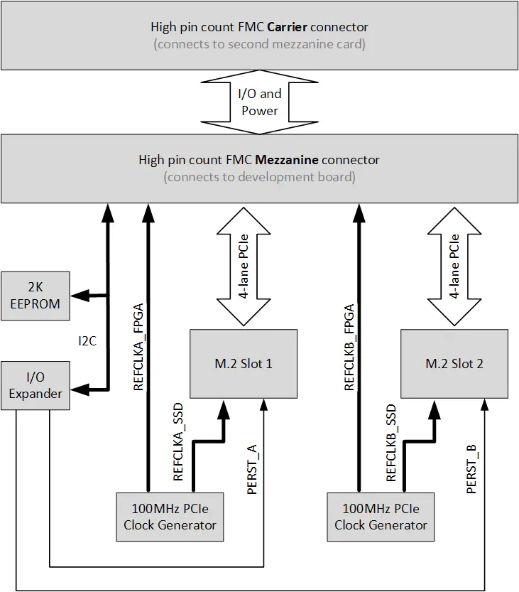
The following I/O signals are passed through to the FMC Carrier connector for use by a second mezzanine card.
Signals common to all FMC cards (LPC, HPC and FMC+):
- LA00-LA33
- CLK0_M2C_P/N, CLK1_M2C_P/N
- VREF_A_M2C
- PG
- JTAG signals: TCK, TDI, TDO, TMS, TRST_L
- GA0, GA1
- I2C_SCL, I2C_SDA
Signals used by HPC and FMC+ cards:
- HA00-HA23
- HB00-HB21
- PG_M2C
- CLK_DIR
- RES0
- VIO_B_M2C_1, VIO_B_M2C_2
- CLK2_BIDIR_P/N, CLK3_BIDIR_P/N
- VREF_B_M2C
PCIe interfaces
The 4-lane PCIe interfaces are routed to FMC pins that are dedicated to gigabit transceivers. The connections are shown in the tables below. Note that in this documentation, the label for the first M.2 module is M.2 Slot 1 while the second is M.2 Slot 2.
M.2 Slot 1
| Direction | PCIe lane | FMC Pin | FMC name | Net name |
|---|---|---|---|---|
| SSD-to-FPGA | 0 | C6/C7 | DP0_M2C_P/N | SSDA2FPGA_0_P/N |
| 1 | A2/A3 | DP1_M2C_P/N | SSDA2FPGA_1_P/N | |
| 2 | A6/A7 | DP2_M2C_P/N | SSDA2FPGA_2_P/N | |
| 3 | A10/A11 | DP3_M2C_P/N | SSDA2FPGA_3_P/N | |
| FPGA-to-SSD | 0 | C2/C3 | DP0_C2M_P/N | FPGA2SSDA_0_P/N |
| 1 | A22/A23 | DP1_C2M_P/N | FPGA2SSDA_1_P/N | |
| 2 | A26/A27 | DP2_C2M_P/N | FPGA2SSDA_2_P/N | |
| 3 | A30/A31 | DP3_C2M_P/N | FPGA2SSDA_3_P/N |
M.2 Slot 2
| Direction | PCIe lane | FMC Pin | FMC name | Net name |
|---|---|---|---|---|
| SSD-to-FPGA | 0 | A14/A15 | DP4_M2C_P/N | SSDB2FPGA_0_P/N |
| 1 | A18/A19 | DP5_M2C_P/N | SSDB2FPGA_1_P/N | |
| 2 | B16/B17 | DP6_M2C_P/N | SSDB2FPGA_2_P/N | |
| 3 | B12/B13 | DP7_M2C_P/N | SSDB2FPGA_3_P/N | |
| FPGA-to-SSD | 0 | A34/A35 | DP4_C2M_P/N | FPGA2SSDB_0_P/N |
| 1 | A38/A39 | DP5_C2M_P/N | FPGA2SSDB_1_P/N | |
| 2 | B36/B37 | DP6_C2M_P/N | FPGA2SSDB_2_P/N | |
| 3 | B32/B33 | DP7_C2M_P/N | FPGA2SSDB_3_P/N |
Reference clocks
The mezzanine card has two clock oscillators ( MicroChip, 2x Output PCIe Clock Generator, DSC557-0334FI1 ), one for each M.2 slot. Each clock oscillator generates two synchronous 100MHz clocks; one LVDS and the other HCSL. The LVDS clocks are fed to the FMC connector, while the HCSL clocks are fed directly to the M.2 slots.
| Synchronous to | FMC Pin | FMC name | Net name |
|---|---|---|---|
| M.2 Slot 1 | D4/D5 | GBTCLK0_M2C_P/N | REFCLKA_FPGA_P/N |
| M.2 Slot 2 | B20/B21 | GBTCLK1_M2C_P/N | REFCLKB_FPGA_P/N |
I2C bus
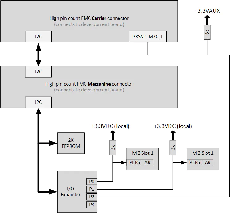
A 2K EEPROM and I/O expander sit on the FMC card’s dedicated I2C bus. The FMC pins of the I2C bus are shown below, and it is up to the user to determine their corresponding connections to the FPGA/MPSoC on the carrier board being used.
| I2C bus signal | FMC pin name | FMC pin number |
|---|---|---|
| SCL (clock) | SCL | C30 |
| SDA (data) | SDA | C31 |
The diagram below illustrates the I2C bus connections and provides more detail of the I/O expander connections.
EEPROM
The EEPROM ( ST, 2K EEPROM, M24C02-FDW6TP ) stores IPMI FRU data that can be read by the carrier board and contains the following information:
- Manufacturer name (Opsero Electronic Design Inc.)
- Product name
- Product part number
- Serial number
- Power supply requirements
The FRU data is read by some carrier boards to determine the correct VADJ voltage to apply to the mezzanine card. All Opsero FMC products have their EEPROMs programmed with valid FRU data to allow these carrier boards to correctly power them.
I/O Expander
The M.2 M-key Stack FMC passes through all of the FMC I/O signals to the second mezzanine card, with the exception of the gigabit transceivers and their associated clocks. The I2C I/O expander ( TI, IO Expander, TCA9536DTMR ) is provided as a means to drive each M.2 module’s reset signal (PERST#), for applications that require this level of control. The PERST# signals are also connected to pull up resistors so that the M.2 modules are released from reset on power up. The I/O expander’s GPIOs all default to inputs on power-up, so most applications will not need to deal with the I/O expander at all.
| PERST_A#/B# | Function |
|---|---|
| 0 (LOW) | M.2 module in reset |
| 1 (HIGH) | M.2 module operational |
Power Supplies
All power required by the M.2 M-key Stack FMC is supplied by the FPGA/MPSoC board through the FMC connector:
- +12VDC
- +3.3VAUX
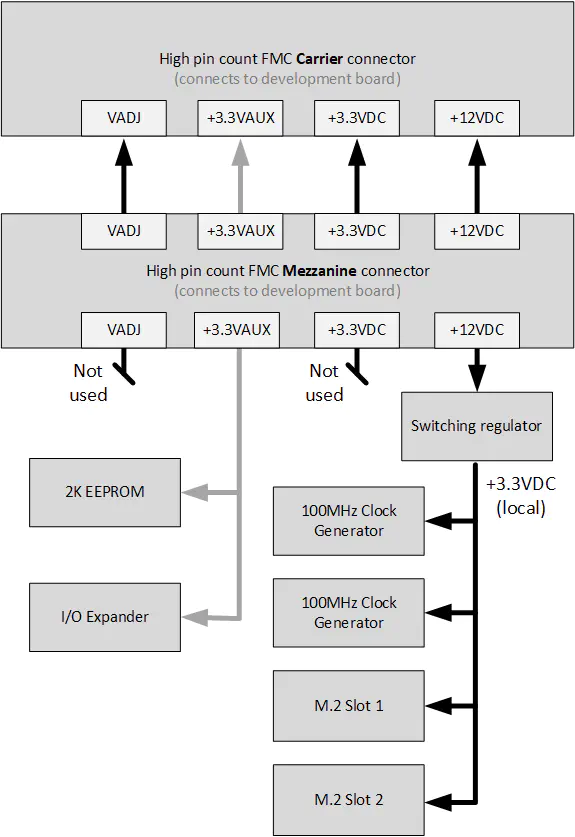
The FPGA/MPSoC carrier board also supplies a 3.3VDC and adjustable (VADJ) power supply, however these are not used by the M.2 M-key Stack FMC. All of the supplies are passed through to the FMC Carrier connector for use by a second mezzanine card.
12VDC Supply
The 12VDC supply is used to power both M.2 modules via a buck switching regulator ( TI, 3-16V 5A Buck Converter, TPS565247DRLR ). The switching regulator converts the 12VDC supply to a 3.3VDC supply which powers both M.2 modules and their corresponding 100MHz clock oscillators.
An LED indicates when power from the switching regulator is active, and it can be seen in the labelled bottom view of the board above.
3.3VAUX Supply
The 3.3VAUX supply is used by the M.2 M-key Stack FMC to power the following devices:
- 2K EEPROM
- I/O Expander
- Inverter
- Bus switch
3.3VDC Supply (FMC)
The 3.3VDC supply from the FPGA/MPSoC board is not used by the M.2 M-key Stack FMC and is passed through to the FMC Carrier connector for use by a second mezzanine card.
3.3VDC Supply (local)
The local 3.3VDC supply that is generated by the buck switching regulator is used to power the two M.2 modules and their respective 100MHz clock oscillators. This 3.3VDC supply is not connected to the FMC provided 3.3VDC, and it is not passed through to the second mezzanine card.
VADJ Supply
The adjustable voltage supply (VADJ), is the I/O voltage that is supplied by all standard FMC carriers. When used without a second mezzanine card, the M.2 M-key Stack FMC can accept any VADJ voltage in the range of 1.2V to 3.3V. The mezzanine card has an onboard FRU EEPROM that specifies acceptance of any VADJ voltage within the range 1.2V to 3.3V. All carriers with a power management system will read this EEPROM on power-up and apply a voltage in the range specified by the EEPROM. Note that some development boards require the VADJ voltage to be configured by a DIP switch or jumper placement, in which case we suggest that it be set to 1.8V.
When the M.2 M-key Stack FMC is used with a second mezzanine card, the address of it’s FRU EEPROM is changed so that the power management system instead reads the FRU EEPROM of the second mezzanine. In this way, the second mezzanine determines the adjustable voltage supply (VADJ) according to it’s needs.
The adjustable voltage supply (VADJ) is not used by the M.2 M-key Stack FMC and is passed through to the FMC Carrier connector for use by a second mezzanine card.
Power LED and testpoints
A single green LED on the mezzanine card is used to indicate when the required power supplies are active. The location of this LEDs can be seen in the labelled bottom view of the board above.
To aid hardware debug, test points are accessible on the bottom side of the mezzanine card for each of the power supplies of the M.2 M-key Stack FMC.