Detailed Description
Hardware Overview
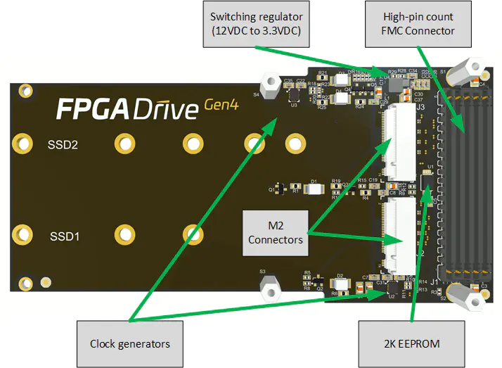
The figure below illustrates the various hardware components that are located on the top-side of the FPGA Drive FMC Gen4.

The main components on the top-side of the mezzanine card are:
- 2x M-key M.2 socket connectors (for the SSDs)
- High Pin Count FMC Connector
- 2K EEPROM
- 2x PCIe Clock oscillators (100MHz)
- Switching regulator
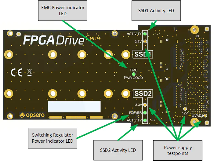
The figure below illustrates the various hardware components that are located on the bottom-side of the mezzanine card.

The main components on the bottom-side of the mezzanine card are:
- FMC Power indicator LED
- Switching regulator power indicator LED
- SSD activity LEDs
- Test points for power supplies
M.2 connectors
The NVMe PCIe SSDs connect to the mezzanine card through 2x M-key M.2 connectors ( Amphenol, PCIe M.2 connector, MDT420M02003 ).
The pinout of the M.2 connector is shown in the table below:
| Pin # | Pin name | Connection | Pin # | Pin name | Connection |
|---|---|---|---|---|---|
| 1 | GND | GND | 2 | 3.3V | 3V3 |
| 3 | GND | GND | 4 | 3.3V | 3V3 |
| 5 | PER-N3 | SSD2FPGA_3_N | 6 | N/C | NC |
| 7 | PER-P3 | SSD2FPGA_3_P | 8 | N/C | NC |
| 9 | GND | GND | 10 | DAS/DSS#/LED1# | DAS/DSS# |
| 11 | PET-N3 | FPGA2SSD_3_N | 12 | 3.3V | 3V3 |
| 13 | PET-P3 | FPGA2SSD_3_P | 14 | 3.3V | 3V3 |
| 15 | GND | GND | 16 | 3.3V | 3V3 |
| 17 | PER-N2 | SSD2FPGA_2_N | 18 | 3.3V | 3V3 |
| 19 | PER-P2 | SSD2FPGA_2_P | 20 | N/C | NC |
| 21 | GND | GND | 22 | N/C | NC |
| 23 | PET-N2 | FPGA2SSD_2_N | 24 | N/C | NC |
| 25 | PET-P2 | FPGA2SSD_2_P | 26 | N/C | NC |
| 27 | GND | GND | 28 | N/C | NC |
| 29 | PER-N1 | SSD2FPGA_1_N | 30 | N/C | NC |
| 31 | PER-P1 | SSD2FPGA_1_P | 32 | N/C | NC |
| 33 | GND | GND | 34 | N/C | NC |
| 35 | PET-N1 | FPGA2SSD_1_N | 36 | N/C | NC |
| 37 | PET-P1 | FPGA2SSD_1_P | 38 | DEVSLP | GND |
| 39 | GND | GND | 40 | SMB_CLK | NC |
| 41 | PER-N0 | SSD2FPGA_0_N | 42 | SMB_DATA | NC |
| 43 | PER-P0 | SSD2FPGA_0_P | 44 | ALERT# | NC |
| 45 | GND | GND | 46 | N/C | NC |
| 47 | PET-N0 | FPGA2SSD_0_N | 48 | N/C | NC |
| 49 | PET-P0 | FPGA2SSD_0_P | 50 | PERST# | PERST# |
| 51 | GND | GND | 52 | CLKREQ# | NC |
| 53 | REFCLK-N | REFCLK_SSD_N | 54 | PEWAKE# | NC |
| 55 | REFCLK-P | REFCLK_SSD_P | 56 | RSVD | NC |
| 57 | GND | GND | 58 | RSVD | NC |
| 67 | N/C | NC | 68 | SUSCLK | NC |
| 69 | PEDET | PEDET | 70 | 3.3V | 3V3 |
| 71 | GND | GND | 72 | 3.3V | 3V3 |
| 73 | GND | GND | 74 | 3.3V | 3V3 |
| 75 | GND | GND |
EEPROM
The EEPROM ( ST, 2K EEPROM, M24C02-FDW6TP ) stores IPMI FRU data that can be read by the carrier board and contains the following information:
- Manufacturer name (Opsero Electronic Design Inc.)
- Product name
- Product part number
- Serial number
- Power supply requirements
The FRU data is read by some carrier boards to determine the correct VADJ voltage to apply to the mezzanine card. All Opsero FMC products have their EEPROMs programmed with valid FRU data to allow these carrier boards to correctly power them.
High Pin Count FMC Connector
The FPGA Drive FMC Gen4 has a high pin count (HPC) FMC (FPGA Mezzanine Card) connector for interfacing with an FPGA or SoC development board. The part number of this connector is Samtec, High pin count FMC connector, Module side, ASP-134488-01 . This HPC FMC connector can be mated with LPC, HPC or FMC+ carrier connectors.
The pinout of this connector conforms to the VITA 57.1 FPGA Mezzanine Card Standard (for more information, see Pin configuration. For more information on the FMC connector and the VITA 57.1 standard, see the Samtec page on VITA 57.1 .
I/O Interfaces
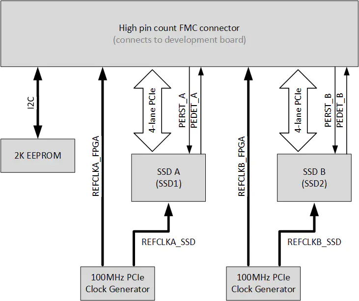
The FMC connector provides power to the FPGA Drive FMC Gen4 and also presents the following I/O signals to the FPGA fabric of the development board:
- 2x 4-lane PCIe interfaces for the SSDs
- 2x PERST active-high reset signals (driven by FPGA)
- 2x PEDET detect signals (driven by mezzanine card)
- 2x LVDS 100MHz PCIe reference clocks
- I2C for EEPROM R/W access
The 2x 4-lane PCIe interfaces are routed to independent gigabit transceivers on the FMC connector for maximum throughput. The figure below illustrates the main connections to the FMC connector. Note that the PERST signals pass through FETs for inversion and level translation, however this circuit is left out of the diagram for clarity.

PCIe interfaces
The 4-lane PCIe interfaces are routed to FMC pins that are dedicated to gigabit transceivers. The connections are shown in the tables below. Note that in this documentation, the label for the first SSD is SSD A (or SSD1) while the second SSD is SSD B (or SSD2).
SSD A (SSD1)
| Direction | PCIe lane | FMC Pin | FMC name | Net name |
|---|---|---|---|---|
| SSD-to-FPGA | 0 | C6/C7 | DP0_M2C_P/N | SSDA2FPGA_0_P/N |
| 1 | A2/A3 | DP1_M2C_P/N | SSDA2FPGA_1_P/N | |
| 2 | A6/A7 | DP2_M2C_P/N | SSDA2FPGA_2_P/N | |
| 3 | A10/A11 | DP3_M2C_P/N | SSDA2FPGA_3_P/N | |
| FPGA-to-SSD | 0 | C2/C3 | DP0_C2M_P/N | FPGA2SSDA_0_P/N |
| 1 | A22/A23 | DP1_C2M_P/N | FPGA2SSDA_1_P/N | |
| 2 | A26/A27 | DP2_C2M_P/N | FPGA2SSDA_2_P/N | |
| 3 | A30/A31 | DP3_C2M_P/N | FPGA2SSDA_3_P/N |
SSD B (SSD2)
| Direction | PCIe lane | FMC Pin | FMC name | Net name |
|---|---|---|---|---|
| SSD-to-FPGA | 0 | A14/A15 | DP4_M2C_P/N | SSDB2FPGA_0_P/N |
| 1 | A18/A19 | DP5_M2C_P/N | SSDB2FPGA_1_P/N | |
| 2 | B16/B17 | DP6_M2C_P/N | SSDB2FPGA_2_P/N | |
| 3 | B12/B13 | DP7_M2C_P/N | SSDB2FPGA_3_P/N | |
| FPGA-to-SSD | 0 | A34/A35 | DP4_C2M_P/N | FPGA2SSDB_0_P/N |
| 1 | A38/A39 | DP5_C2M_P/N | FPGA2SSDB_1_P/N | |
| 2 | B36/B37 | DP6_C2M_P/N | FPGA2SSDB_2_P/N | |
| 3 | B32/B33 | DP7_C2M_P/N | FPGA2SSDB_3_P/N |
Reference clocks
The mezzanine card has two clock oscillators ( MicroChip, 2x Output PCIe Clock Generator, DSC557-0334FI1 ), one for each SSD. Each clock oscillator generates two synchronous 100MHz clocks; one LVDS and the other HCSL. The LVDS clocks are fed to the FMC connector, while the HCSL clocks are fed directly to the SSDs.
| Synchronous to | FMC Pin | FMC name | Net name |
|---|---|---|---|
| SSD A | D4/D5 | GBTCLK0_M2C_P/N | REFCLKA_FPGA_P/N |
| SSD B | B20/B21 | GBTCLK1_M2C_P/N | REFCLKB_FPGA_P/N |
PERST
The PERST_A and PERST_B signals are active-high reset signals of SSD A and SSD B respectively, and they are driven by the FPGA. The FPGA drives these signals at VADJ voltage levels, while the SSDs require 3.3VDC active-low signals. For this reason, the mezzanine card has two FET based inverter circuits to perform the level translation and the signal inversion. The FPGA design should drive these signals active-high as shown in the table below:
| PERST_A/B | Function |
|---|---|
| 0 (LOW) | SSD operational |
| 1 (HIGH) | SSD in reset |
PEDET
The PEDET_A and PEDET_B signals are outputs of the mezzanine card and they can be read by the FPGA if so desired. The purpose of the signal is to indicate whether the connected SSD has a PCIe or SATA interface. The functionality of the output is described in the table below:
| PEDET_A/B | Function |
|---|---|
| 0 (LOW) | SATA |
| 1 (HIGH) | PCIe |
This signal is not used in our example designs and is not required if only using NVMe PCIe SSDs.
Power Supplies
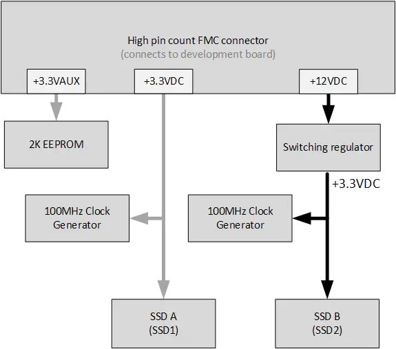
All power required by the FPGA Drive FMC Gen4 is supplied by the development board through the FMC connector:
- +12VDC
- +3.3VDC
- +3.3VAUX (for powering EEPROM only)
- VADJ: +1.8VDC
The mezzanine card powers the first SSD and it’s clock generator using the FMC’s 3.3VDC supply. It has a switching regulator to power the second SSD and it’s clock generator using the FMC’s 12VDC supply.

12VDC Supply
The 12VDC supply is used to power the second SSD (SSD B/SSD2) via a buck switching regulator ( TI, 3-17V 2-3A Buck Converter, TPS62913RPUR ). The switching regulator converts the 12VDC supply to a 3.3VDC supply which powers SSD B (SSD2) and its corresponding 100MHz clock oscillator. The switching regulator can be disabled by driving the DISABLE_SSD2_PWR pin as described in the table below:
| DISABLE_SSD2_PWR | Function |
|---|---|
| 0 (LOW) | SSD B power enabled |
| 1 (HIGH) | SSD B power disabled |
The DISABLE_SSD2_PWR is controlled via the LA07_P pin of the FMC connector. The mezzanine card has a pull down resistor to hold this pin to ground, enabling the switching regulator, if it is not driven by the FPGA.
An LED indicates when the switching regulator is enabled (ie. when SSD B has power), and it can be seen in the labelled bottom view of the board above.
3.3VDC Supply
The 3.3VDC supply provides power for the first SSD (SSD A/SSD1) and the corresponding 100MHz clock oscillator.
VADJ Supply
The adjustable voltage supply (VADJ), is the I/O voltage that is supplied by all standard FMC carriers. The FPGA Drive FMC Gen4 can accept any VADJ voltage in the range of 1.2V to 3.3V. The mezzanine card has an onboard FRU EEPROM that specifies acceptance of any VADJ voltage within the range 1.2V to 3.3V (see note below). All carriers with a power management system will read this EEPROM on power-up and apply a voltage in the range specified by the EEPROM. Note that some development boards require the VADJ voltage to be configured by a DIP switch or jumper placement, in which case we suggest that it be set to 1.8V.
Power LED and testpoints
Two red LEDs on the mezzanine card are used to indicate when the required power supplies are active. The location of these LEDs can be seen in the labelled bottom view of the board above. The main LED in the middle of the board indicates when the FMC’s 12VDC, 3.3VDC and VADJ voltages are active. The second LED indicates when the 3.3VDC supply generated by the switching regulator is active (ie. when the second SSD is powered).
To aid hardware debug, test points are accessible on the bottom side of the mezzanine card for each of the power supplies of the FPGA Drive FMC Gen4.